In today’s modern technology world, we constantly hear about powerful semiconductor chips. These chips power supercomputers, smartphones, AI systems, and even autonomous vehicles. However, before a chip becomes fully functional, the silicon wafer must undergo an extremely complex manufacturing journey. This journey is known as the Front-End Process (Wafer Fabrication).
This stage is considered the “heart” of the semiconductor industry. At the same time, it requires atomic-level precision. Therefore, leading semiconductor manufacturers rely heavily on advanced vacuum and surface processing technologies.
In this field, ULVAC is recognized as one of Japan’s leading vacuum technology companies. Today, ULVAC plays a critical role in the global Front-End semiconductor manufacturing supply chain.
Let’s explore the cleanroom environment with ULVAC and discover how engineers transform ordinary quartz sand into the “brains” of the digital era.
1. What is the Front-End Process?
If semiconductor manufacturing is compared to constructing a skyscraper, the Front-End process represents the foundation and structural framework of the building.
The Front-End stage, also known as Wafer Fabrication or Wafer Fab, includes all physical and chemical processes performed directly on silicon wafers. The objective is to create billions of transistors and ultra-fine circuit patterns on a single wafer surface.
This is the most complicated stage in semiconductor production. According to industry experts, Front-End processing can account for nearly 70% of total semiconductor manufacturing costs. 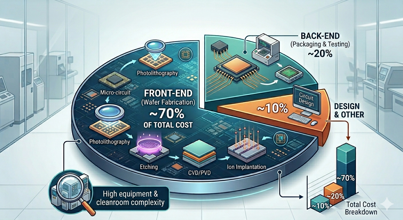
In addition, the entire process must be carried out inside ultra-clean environments that meet Cleanroom Class 1 standards. This minimizes contamination from microscopic particles and impurities.
2. Core Steps in the Front-End Process and the Role of ULVAC
A silicon wafer must go through hundreds of repeated process cycles. Depending on chip complexity, the number of process steps may increase significantly.
Below are the key stages of the Front-End semiconductor manufacturing process.
Step 1: Preparation of Ultra-Pure Silicon Wafer
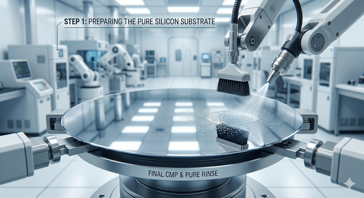
Everything begins with quartz sand. After extensive purification, silicon reaches an extremely high purity level of up to 99.9999999%.
The silicon is then melted and pulled into cylindrical ingots. Next, the ingots are sliced into thin wafers.
Finally, the wafers are polished to a mirror-like finish. This creates an ideal surface for semiconductor circuit formation.
The wafer quality at this stage directly impacts final chip performance. Therefore, strict flatness and cleanliness standards are required.
Step 2: Oxidation and Annealing
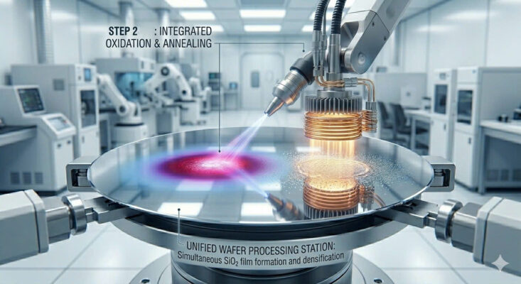
Next, the wafer is placed inside a high-temperature furnace. The purpose is to form an ultra-thin silicon dioxide ($SiO_2$) layer on the wafer surface.
This oxide layer acts as an essential insulating layer within semiconductor transistors.
ULVAC Solution
ULVAC provides advanced Rapid Thermal Processing (RTA) systems. These systems offer highly accurate temperature control.
Furthermore, ULVAC technology improves oxide layer uniformity while maintaining wafer structural stability during heating.
As a result, semiconductor manufacturers can reduce structural distortion at nanometer-scale dimensions.
Step 3: Photolithography – Printing Circuit Patterns
Photolithography is one of the most important stages in semiconductor fabrication.
During this process, DUV or EUV ultraviolet light passes through a photomask to transfer circuit patterns onto the photoresist-coated wafer surface.
This step determines transistor density on the chip. Therefore, nanometer-level precision is essential.
Today, EUV technology plays a key role in manufacturing advanced AI chips and high-performance processors.
Step 4: Dry Etching and Ashing
After photolithography, excess material must be removed to form permanent circuit structures on the wafer.
Previously, wet chemical etching methods were widely used. However, they often caused dimensional inaccuracies at smaller technology nodes.
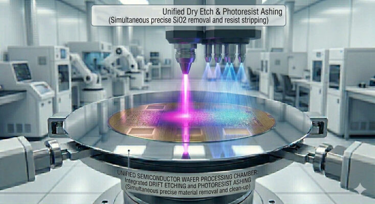
Today, Plasma Dry Etching is preferred because of its superior precision.
ULVAC Solution
ULVAC provides advanced Plasma Etching and Ashing systems. Its ultra-high vacuum technology enables highly precise material removal. 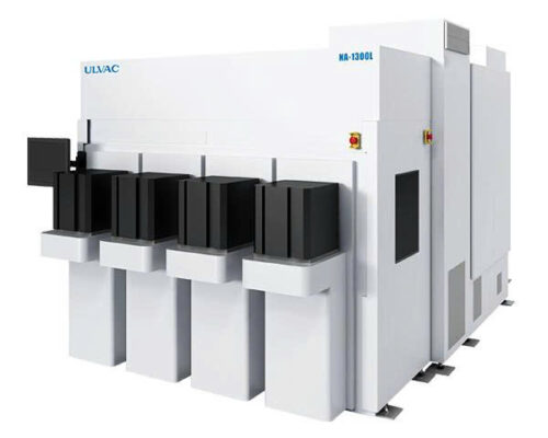
More importantly, the system minimizes damage to underlying wafer structures.
In addition, ULVAC’s Ashing technology efficiently removes photoresist residues and reduces wafer contamination risks.
Step 5: Ion Implantation
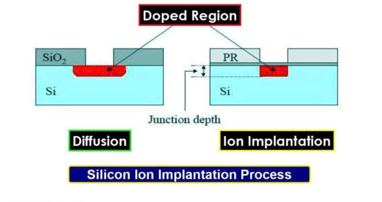
At this stage, ions such as Boron or Phosphorus are implanted into selected wafer regions.
This process modifies the electrical conductivity of silicon, enabling transistors to function properly.
Ion Implantation is considered a foundational process in modern semiconductor device fabrication.
Moreover, the accuracy of this step directly affects chip performance and power consumption.
Step 6: Thin Film Deposition – ULVAC’s Core Technology Strength
This is one of the most critical stages in the Front-End process.
To electrically connect billions of transistors, conductive and insulating thin films must be deposited onto the wafer surface. These films are often only a few nanometers thick.
Common materials include:
- Copper (Cu)
- Aluminum (Al)
- Titanium (Ti)
- Titanium Nitride (TiN)
- Silicon Nitride
ULVAC’s Leadership Position
ULVAC is recognized as a leading supplier of PVD and CVD technologies.
ULVAC’s Physical Vapor Deposition (PVD) and Chemical Vapor Deposition (CVD) systems provide thin films with:
- Excellent uniformity
- Strong adhesion
- Low contamination levels
- Stable vacuum process performance
These factors are essential for semiconductor chip performance, reliability, and lifespan.
Additionally, advanced thin film technologies help optimize conductivity and reduce electrical resistance in integrated circuits.
3. Defect Inspection and Leak Testing After Front-End Processing
Before wafers proceed to the Back-End stage, they must undergo rigorous inspection procedures. 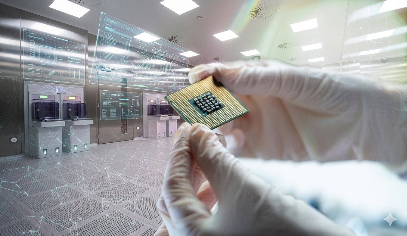
Engineers must ensure:
- No circuit defects
- No gas leakage
- No contamination inside vacuum chambers
If defects are discovered at this stage, manufacturing losses can become extremely costly.
ULVAC Inspection Systems
ULVAC provides highly sensitive Helium Leak Detectors.
These systems can detect microscopic leaks in processing chambers or wafer surfaces. As a result, manufacturers can significantly reduce defect rates before wafer dicing and packaging.
In addition, advanced vacuum inspection technologies improve production stability for high-volume semiconductor manufacturing lines.
4. ULVAC Vietnam – Supporting the Semiconductor Industry
Today, Vietnam’s semiconductor industry is experiencing rapid growth. Many global technology companies are expanding their investments in the country.
As a result, demand for vacuum systems and thin film technologies continues to rise.
ULVAC Vietnam proudly provides:
- Genuine Japanese vacuum equipment
- Advanced PVD/CVD systems
- High-precision Plasma Etching systems
- International-standard maintenance services
- High-quality spare parts
- Professional technical support engineers
Furthermore, ULVAC Vietnam offers specialized consulting solutions for semiconductor cleanrooms and advanced manufacturing facilities.
Q&A – Front-End Semiconductor Manufacturing Process
1. What is the Front-End process in semiconductor manufacturing?
The Front-End process is the wafer fabrication stage where transistors and integrated circuits are formed on silicon wafers.
2. Why does Front-End manufacturing require vacuum technology?
Vacuum technology minimizes contamination, improves precision, and protects wafers in ultra-clean manufacturing environments.
3. What are PVD and CVD used for?
PVD and CVD are used to deposit conductive and insulating thin films onto semiconductor wafers.
4. What is Plasma Etching?
Plasma Etching is a dry etching technology used to create highly precise nanometer-scale circuit structures.
5. Why is leak testing important?
Leak testing helps identify vacuum system defects and reduces wafer failure rates.
6. Does Vietnam have strong semiconductor industry potential?
Yes. Vietnam is attracting significant investment in semiconductor manufacturing, electronics, and high-tech industries.
Conclusion
The Front-End process forms the technological foundation of modern semiconductor manufacturing. It is where innovative ideas are transformed into functional semiconductor devices on ultra-thin silicon wafers.
To achieve atomic-level precision, manufacturers require advanced vacuum and thin film processing technologies.
With decades of experience in industrial vacuum and semiconductor technologies, ULVAC continues to strengthen its position as a trusted technology partner for manufacturers worldwide.
Contact ULVAC Vietnam today to receive expert consultation on vacuum technology solutions, PVD/CVD systems, and advanced semiconductor manufacturing equipment.