In the era of high technology, the continuous scaling down of semiconductor device dimensions has become a key factor in enhancing computing performance while reducing power consumption in smart electronic devices. As a result, advanced thin-film technology is playing an increasingly critical role in modern wafer manufacturing. 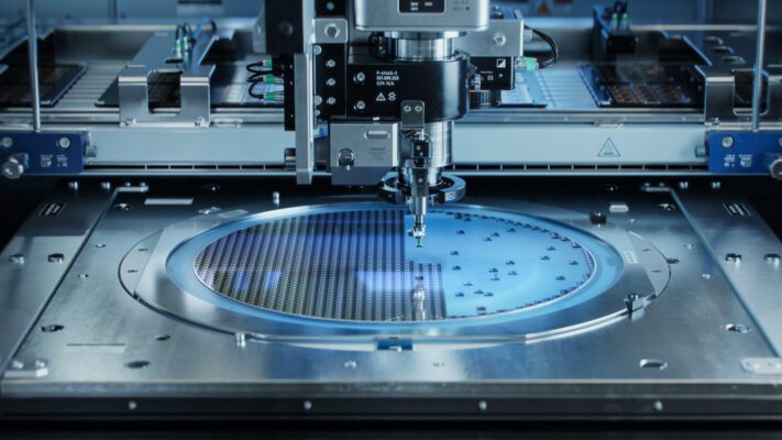
As a global pioneer in vacuum and thin-film technologies, ULVAC continues to support the semiconductor industry with advanced deposition solutions. In particular, Metal Hard Mask (MHM) deposition technology is emerging as a strategic solution for next-generation semiconductor manufacturing processes.
With this technology, manufacturers can achieve ultra-fine integrated circuit patterns with extremely high precision. At the same time, it meets the increasingly stringent requirements of advanced scaling processes.
1. What is MHM? A Core Technology for Advanced Etching Processes 
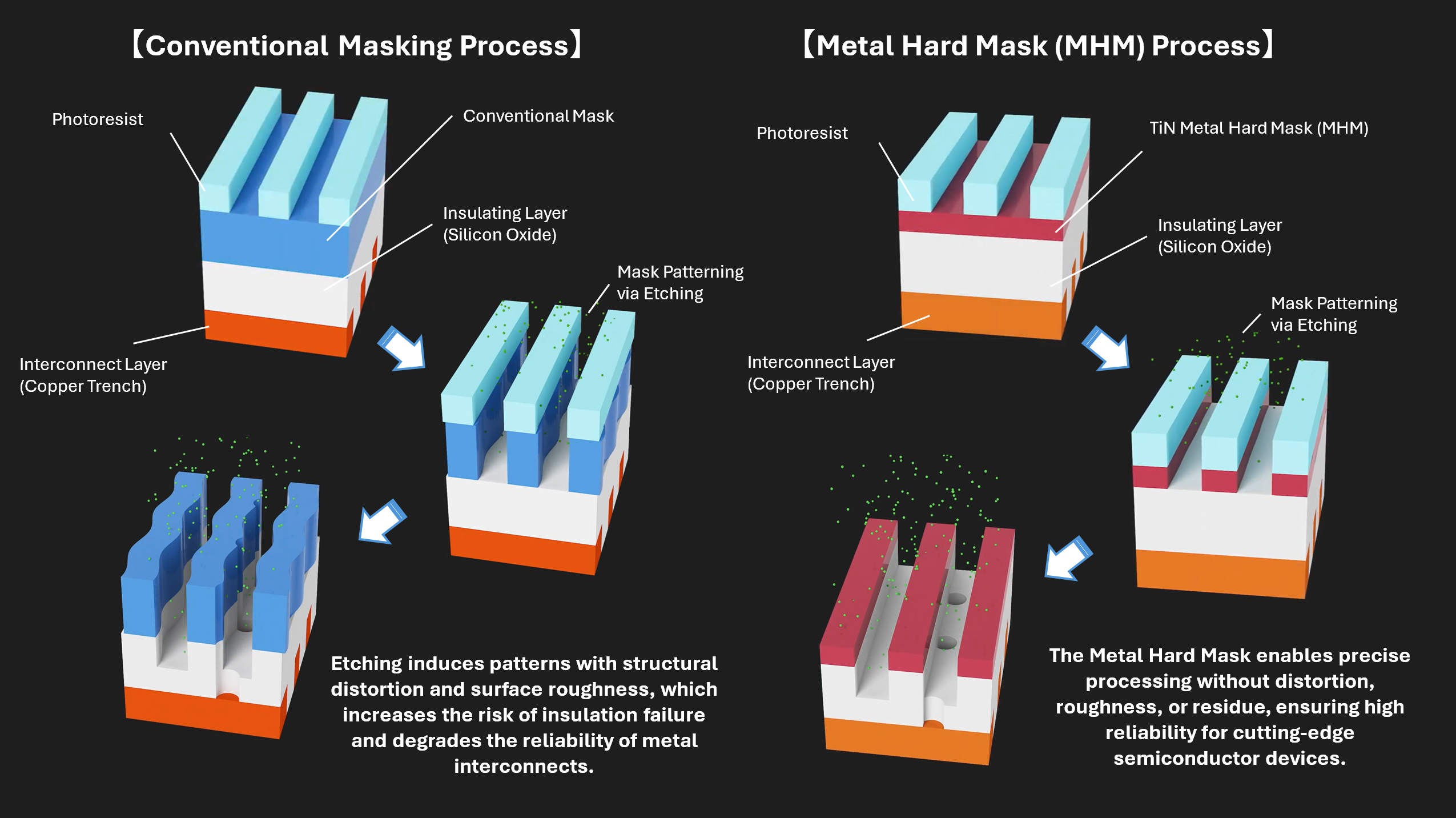
MHM (Metal Hard Mask) is a specialized metal thin film used as a “hard mask” during the etching process in semiconductor manufacturing. This layer helps protect and precisely define ultra-fine circuit patterns on the wafer.
In conventional photolithography, photoresist—a light-sensitive material—is directly used as a temporary mask to transfer circuit patterns onto the silicon wafer.
However, as semiconductor technology advances toward smaller nodes, the depth and sharpness of etched features increase significantly. As a result, conventional photoresists can no longer withstand high-energy plasma environments.
This leads to:
- Mask erosion
- Pattern deformation
- Reduced patterning accuracy
To overcome these limitations, manufacturers introduce an additional ultra-durable metal layer beneath the photoresist—this is the MHM layer.
Initially, the photoresist defines the pattern for the metal layer. Then, the hard metal layer becomes the primary mask for the core deep etching process.
By utilizing materials with superior hardness, engineers can fabricate nanoscale structures with extremely high precision.
The Role of MHM in Advanced Semiconductor Technology
Today, MHM is considered a foundational technology for:
- EUV lithography processes
- Advanced logic chips
- Next-generation memory
- High-performance image sensors
In addition, it improves the stability of etching processes in structures with extremely high transistor density. Therefore, MHM is becoming an almost indispensable solution in modern semiconductor fabs.
This is also one of the core technological capabilities that enables ULVAC to collaborate with leading semiconductor manufacturers worldwide.
2. Why is MHM Becoming a Key Trend in the Semiconductor Industry?
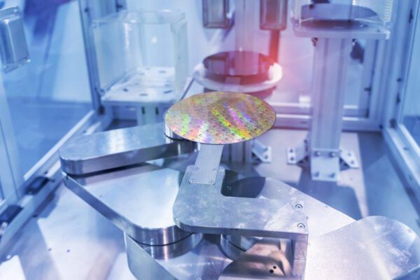
The semiconductor industry is no longer focused solely on increasing transistor density. Instead, the entire industry is moving toward:
- Smaller circuit structures
- Higher processing speeds
- Lower power consumption
However, as transistor dimensions shrink, plasma etching processes become more complex. At the same time, high aspect ratio structures require masks with:
- Extremely high durability
- Strong plasma resistance
- Absolute geometric stability
Even the slightest deformation of the mask can significantly impact wafer yield. As a result, advanced MHM technologies are being heavily invested in next-generation semiconductor fabs.
Expanding Applications of MHM Technology
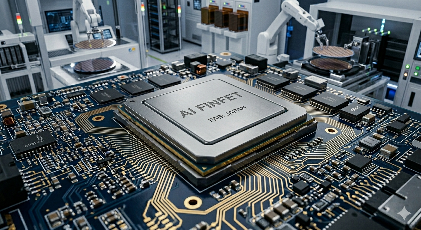
Today, demand for MHM deposition technology is rapidly growing in:
- AI chips
- High-performance computing (HPC)
- Advanced memory
- Image sensors
- Optoelectronic devices
- VCSEL components
Furthermore, the rapid growth of AI and data centers is driving strong demand for ultra-precise patterning technologies.
3. ULVAC’s Strength: Proprietary Thin Film Stress Control Technology
One of the standard materials used in MHM structures is TiN (Titanium Nitride), known for its exceptional hardness and superior plasma resistance. 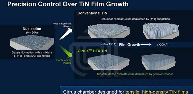
However, TiN also presents a significant technical challenge.
Typically, when depositing high-density TiN films, strong compressive stress is generated, causing the film to contract inward.
In semiconductor manufacturing, excessive film stress poses serious risks, including:
- Wafer warpage
- Film cracking
- Collapse of microstructures
- Reduced production yield
Therefore, precise control of film stress is a critical requirement in advanced processes.
ULVAC’s Technological Breakthrough
To meet increasingly demanding customer requirements, ULVAC has successfully developed a high-density TiN film technology that maintains tensile stress.
This is considered a major breakthrough in MHM deposition technology.
To achieve this, ULVAC has optimized:
- Equipment hardware design
- Plasma conditions
- Process parameters
- Nanoscale crystal orientation control
As a result, customers can finely tune and balance film stress without compromising:
- Film thickness
- Film density
- Plasma resistance performance
More importantly, the ability to precisely control the physical properties of thin films according to specific requirements is a key advantage that positions ULVAC as a strategic partner for leading semiconductor companies worldwide.
4. Future Outlook of MHM Technology
Since its commercialization, MHM technology has rapidly become a major growth driver in ULVAC’s semiconductor equipment business.
Today, its applications extend beyond advanced EUV logic chips into a wide range of fields, including:
- Next-generation memory
- Image sensors
- Optoelectronic devices
- VCSEL devices
- High-performance AI chips
In addition, the growth of AI, high-performance computing, and global data centers continues to drive demand for advanced thin-film deposition technologies.
ULVAC’s Commitment to Innovation
In this context, ULVAC continues to focus on:
- Next-generation deposition technologies
- Advanced vacuum process solutions
- Process stability optimization
- Improving wafer yield for global customers
At the same time, the company continues to invest in new material research to support future generations of chips with higher transistor densities.
ULVAC Vietnam: Supporting the Next Wave of Semiconductor Innovation
In Vietnam, investment in the semiconductor supply chain is accelerating rapidly. As a result, demand for:
- Vacuum technology
- Thin-film equipment
- Advanced deposition processes
- High-precision wafer processing solutions
is growing significantly.
With strong technological expertise and support from its Japanese headquarters, ULVAC Vietnam is committed to delivering:
- Advanced vacuum equipment solutions
- In-depth technical support
- Modern thin-film technology transfer
- Optimized semiconductor manufacturing processes
Contact ULVAC Vietnam’s expert team today to receive tailored solutions for your production line.