In the semiconductor industry, especially in Front-End processes such as Dry Etching, thin film deposition (CVD/ALD), and Ion Implantation, an Ultra-High Vacuum (UHV) environment is absolutely critical. Even a nano-scale gas leak smaller than 10⁻⁹ mbar·L/s can damage an entire wafer worth hundreds of thousands of dollars.
In other words, this is an extremely tiny leak level. Even a minute amount of gas can compromise the purity of the process chamber. Therefore, modern semiconductor fabs consider leak control one of the most important standards for maintaining Yield and Uptime.
So, how do engineers detect these “invisible” leaks? Let’s explore the Helium leak detection technology currently used in the world’s leading semiconductor factories. 
1. Why Conventional Leak Testing Methods Fail
When chamber pressure does not reach the target level or abnormal Pressure Rise occurs, many engineers first think about traditional leak testing methods. However, at the nano-leak level, these methods are no longer effective.
For example:
- Soap bubble testing only works for large leaks.
- Differential pressure testing has limited sensitivity.
- Conventional tracer methods are easily affected by noise in UHV environments.
In practice, the maximum sensitivity of these methods is typically only:
10⁻⁴ to 10⁻⁵ mbar·L/s
Meanwhile, semiconductor manufacturing requires leak detection at far smaller levels.
In addition, common background gases such as:
- Nitrogen (N₂)
- Oxygen (O₂)
have larger molecular sizes than Helium. As a result, they cannot easily pass through nano-scale cracks in welds or microscopic mechanical structures.
Therefore, the global standard today is:
Helium Leak Detection using Helium (He) as the tracer gas.
2. Why Is Helium the Ideal Tracer Gas?
Helium was not chosen by accident. This gas possesses several properties that make it nearly perfect for ultra-small leak detection. 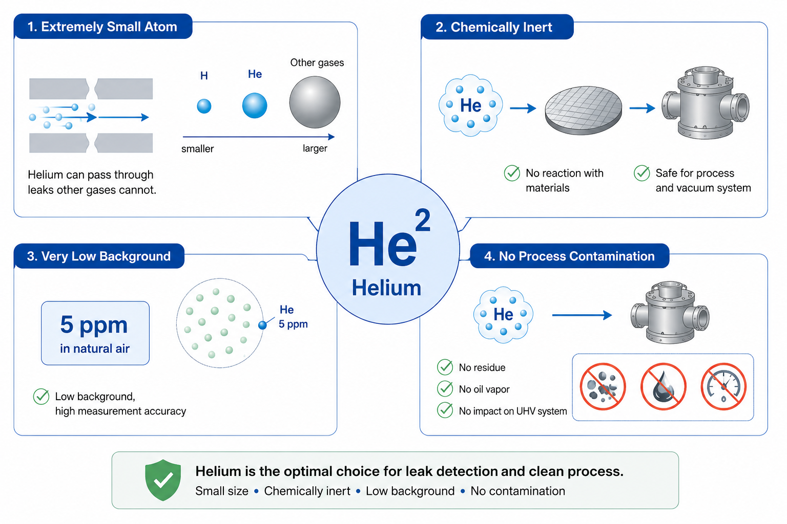
Extremely Small Atomic Size
Helium is the second-smallest atom in nature, just behind Hydrogen. Because of this, Helium can pass through microscopic leaks that other gases cannot penetrate.
Chemically Inert
Helium does not react with wafers, vacuum chamber materials, or process chemicals. Therefore, it is completely safe for semiconductor cleanroom environments.
Very Low Background Concentration
The natural concentration of Helium in the atmosphere is only:
5 ppm
This significantly reduces background noise and improves measurement accuracy.
No Process Contamination
In addition, Helium leaves no residue, produces no oil vapor, and does not affect ultra-high vacuum systems.
3. Helium Spray Method for Detecting Nano Leaks
In semiconductor fabs, the most common technique is the Helium Spray Method. This method uses atmospheric pressure outside the chamber and vacuum conditions inside the chamber.
The operating principle is as follows:
[Helium Spray Gun] ---> (Leak Point on Chamber Surface)
                                 |
+------------------------------------------------------+
|            Semiconductor Vacuum Chamber             |
+------------------------------------------------------+
                                 |
                                 v
                  [Helium Leak Detector]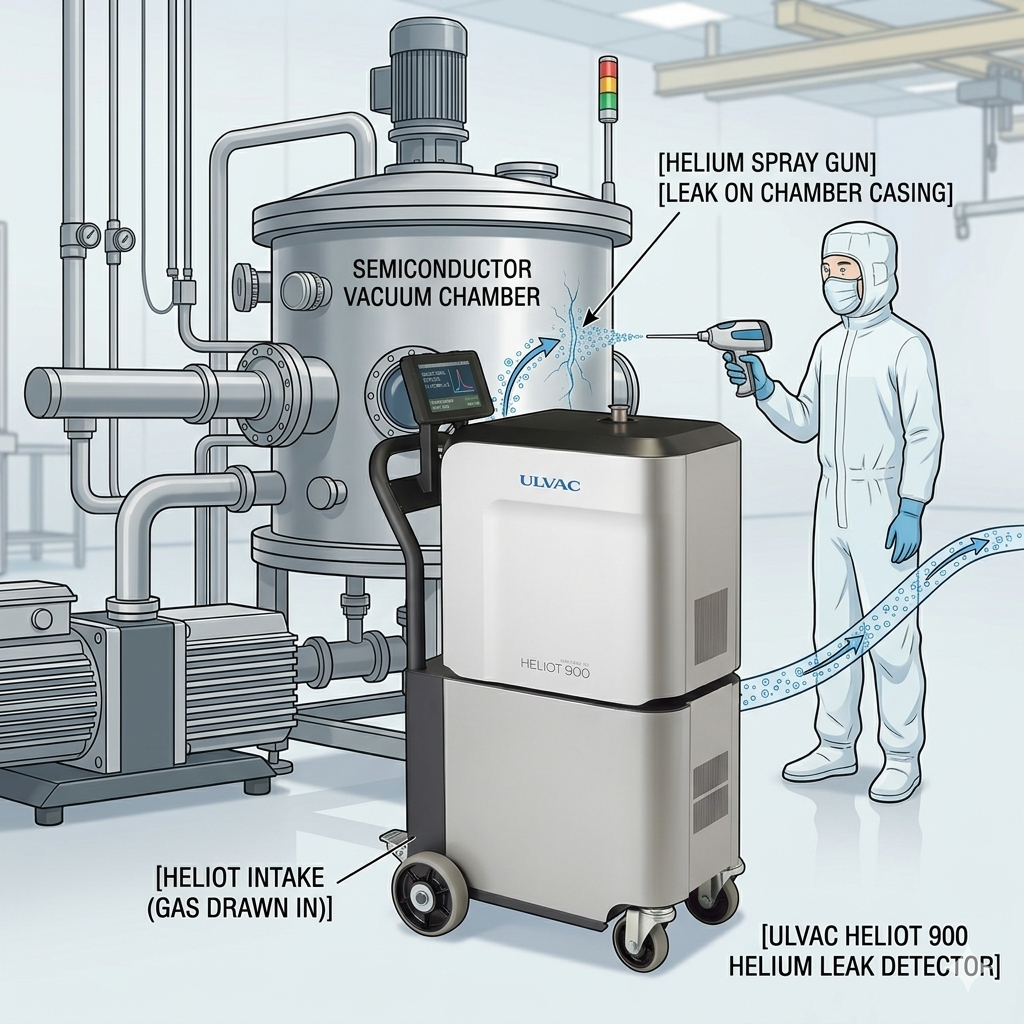
Step 1: Pump Down the System
First, engineers connect the Helium leak detector to the vacuum system.
Typically, the detector is connected:
- in parallel with the vacuum chamber
- or in series after the Turbo Molecular Pump
Next, the chamber is evacuated to the standard testing pressure:
P < 10⁻¹ mbar
The lower the pressure, the higher the leak detection sensitivity.
Step 2: Activate Fine Test Mode
Next, engineers activate the ultra-sensitive measurement mode on the leak detector.
At this stage, the ambient Helium background level must be minimized. The ideal value is typically below:
10⁻¹⁰ mbar·L/s
If the background Helium concentration is too high, the measurement signal becomes noisy and accurate leak localization becomes difficult.
Step 3: Spray Helium Correctly
After the system stabilizes, engineers use a handheld Helium spray gun to scan critical locations.
These areas include:
- flanges
- O-rings
- plasma welds
- electrical feedthroughs
- pressure sensor ports
- gas line fittings
However, the spray sequence is extremely important.
Engineers must always spray:
- from top to bottom
- from near to far
This is because Helium is lighter than air. If engineers spray lower areas first, the gas will rise upward and interfere with measurements at higher positions.
This is one of the most common mistakes during leak testing of large vacuum chambers.
Step 4: Analyze the Helium Signal
When Helium reaches the actual leak point, it is immediately drawn into the vacuum chamber.
The gas then travels into the detector’s mass spectrometer.
Inside the detector, Helium ions with: m/z = 4 are separated by a magnetic field.
Finally, the ion collector detects the signal and triggers an alarm instantly.
4. Technical Pitfalls When Measuring Leaks Below 10⁻⁹ mbar·L/s
Leak detection at the nano scale requires more than just advanced equipment. Engineers also need practical experience.
Below are the most common issues.
Permeation Through Seals
At ultra-sensitive levels, Helium can permeate through rubber seal materials such as Viton.
If engineers spray Helium too long at one location, the detector signal may gradually increase. However, this does not always indicate a real leak.
Experienced engineers usually distinguish them as follows:
Real Leak
- Signal rises rapidly
- Sharp signal increase
- Signal drops quickly after spraying stops
Permeation
- Signal rises slowly
- Signal curve stretches over time
- Longer recovery time
“Clouding” Effect
If the spray gun flow rate is too high, Helium may surround the entire chamber area.
In this situation:
- the detector still indicates a leak
- but engineers cannot identify the exact location
Therefore, Helium flow must always be carefully controlled.
Virtual Leaks
Besides actual leaks, vacuum systems can also experience “Virtual Leaks.”
This occurs when gas becomes trapped inside:
- screw threads
- narrow mechanical gaps
- dead zones inside the chamber
- poorly designed weld structures
Over time, the trapped gas slowly escapes and behaves like a real leak.
As a result, engineers must clearly distinguish between:
- real leaks
- outgassing
- virtual leaks
to avoid unnecessary component replacement.
5. ULVAC Helium Leak Detection Solutions for the Semiconductor Industry
As a global leader in vacuum technology from Japan, ULVAC provides specialized Helium leak detectors for semiconductor and display manufacturing industries. 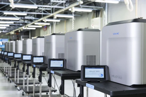
ULVAC HELIOT Series
The HELIOT series is specifically designed for modern semiconductor fabs. These systems meet extremely strict requirements for sensitivity, stability, and cleanliness.
Ultra-High Sensitivity
Some models, such as HELIOT 900, can detect leaks as small as: 10⁻¹² mbar·L/s
As a result, detecting leaks at: 10⁻⁹ mbar·L/s
becomes much faster and more accurate.
High Helium Pumping Speed
Thanks to ULVAC’s advanced vacuum pump technology, the systems provide:
- fast response time
- short recovery time
- rapid signal cleanup
This significantly reduces inspection time for large-volume vacuum chambers.
Cleanroom-Compatible Design
The systems operate quietly, generate minimal vibration, and produce no fine particles.
In addition, the compact design allows engineers to move easily between semiconductor equipment such as:
- lithography systems
- plasma etchers
- ALD/CVD systems
- ion implantation systems
Smart Inspection Features
Key features include:
- Auto Calibration
- real-time graph display
- automatic alarms
- inspection data logging
- leak trend analysis support
As a result, engineers can reduce operational errors and standardize maintenance procedures.
Conclusion
Controlling gas leaks below:
10⁻⁹ mbar·L/s
is not just a technical requirement. It is a critical factor that directly affects Yield, Uptime, and the stability of the entire semiconductor production line.
In modern chip manufacturing environments, even a tiny amount of gas contamination can cause:
- wafer contamination
- thin film defects
- plasma instability
- reduced vacuum equipment lifetime
Therefore, investing in high-sensitivity Helium leak detection systems such as the HELIOT series from ULVAC is essential for next-generation semiconductor fabs.
Are you experiencing vacuum pressure instability or looking to optimize your semiconductor leak testing process?
Contact the engineering team at ULVAC for consultation, on-site equipment demonstrations, and international-standard leak testing solutions.