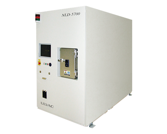
A plasma dry‑etching system is a critical tool in the manufacturing of integrated circuits and electronic components.
Etching, the process of forming grooves and patterns on a wafer surface, has traditionally used wet chemicals. However, dry etching with plasma or reactive gases has become the mainstream choice.
 |  |
1. Plasma Generation
In a vacuum etch chamber, a plasma—a partially ionized gas—comprising ions, electrons, and radicals, is generated.
Application of RF (radio frequency) power or high-voltage discharge to process gases (e.g., CF₄, SF₆, Cl₂, O₂) ionizes these gases into a reactive plasma.
2. Wafer Loading
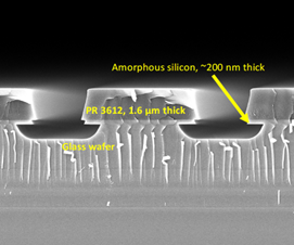
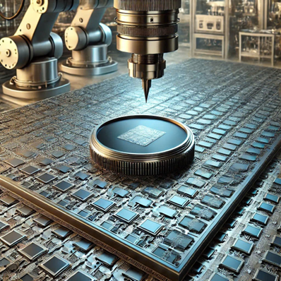
The silicon wafer, pre-coated with photoresist or other masking materials, is placed inside the vacuum chamber to shield areas from etching.
Evacuating the chamber minimizes contamination and ensures process control.
3. Plasma‑Wafer Interaction
Ion etching: Plasma ions are accelerated toward the wafer under an electric field, physically sputtering material vertically to remove unwanted layers.
Chemical etching: Radical species chemically react with target materials (e.g., silicon oxide, nitride, polysilicon), forming volatile byproducts that are evacuated from the chamber.
The combination of physical sputtering and chemical reaction enables atomic‑scale precision.
4. Process Parameter Control
Critical parameters include:
RF power and frequency – higher power increases plasma density.
Chamber pressure – lower pressure yields greater anisotropy and fewer side reactions.
Gas composition and flow ratios – e.g., CF₄/O₂ mixtures tailor the etch chemistry.
Fine-tuning these allows precise control over etch rate, profile, and selectivity.
5. Selective Etching
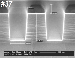
Protected by photoresist, certain wafer regions remain intact while exposed areas are etched, enabling the formation of micro‑structures, vias, and interconnect features with sub‑µm accuracy.
6. Post‑Etch Photoresist Removal
After etching, the photoresist layer is stripped—typically via solvent wash or thermal processing—to reveal clean, finely-patterned wafer surfaces suitable for subsequent processing.
Common Plasma Dry‑Etch Techniques in Semiconductors
Reactive Ion Etching (RIE): Combines directional ion bombardment with chemical reactivity for high-resolution pattern transfer.
Deep Reactive Ion Etching (DRIE): An enhanced RIE variant delivering deep, smooth sidewalls—vital for MEMS fabrication.
Inductively Coupled Plasma (ICP) Etching: Utilizes high-power RF induction to generate dense plasma, enabling uniform and efficient etching across the wafer.
Advantages of Plasma Dry‑Etching
High precision: Enables fabrication of ultra-fine, high-aspect-ratio features essential for modern microelectronics.
Sharp pattern fidelity: Produces well-defined edges with minimal undercutting.
Eliminates liquid waste: Reduces environmental and handling hazards associated with wet chemistry.
Process control: Gas flow, pressure, and RF tuning enable tight reproducibility and customization.
Conclusion
A plasma-based dry-etching system operates by generating a reactive plasma in vacuum, where ions and radicals selectively remove material from a patterned wafer. This technology is indispensable in producing the highly-miniaturized and intricate structures found in contemporary semiconductor and IC manufacturing.